Quantcast
Channel: my tech blog » PCI express
Viewing all 30 articles
Browse latest View live

Getting the PCIe of Avnet S6LX150T Development Kit detected

$
0
0

About a year ago, I had a client failing to get the PCIe working on an Avnet LX150T development board. Despite countless joint efforts, we failed to get the card detected as a PCIe device by the computer.

A recent comment from another client supplied the clue: The user guide (which I downloaded recently from Avnet) is simply wrong about the DIP switch setting of the board. Table 5 (page 11) says that SW8 should be set OFF-ON-OFF to have a reference clock of 125 MHz to the FPGA.

On the other hand, Avnet’s AXI PCIe Endpoint Design guide for the same board (also downloaded recently from Avnet) says on page 30, that the setting for the same frequency should be ON-ON-ON.

Hmmm… So which one is correct?

Well, those signals go to an IDT ICS874003-05 PCI Express jitter attenuator, which consists of a frequency synthesizer. It multiplies the board’s 100 MHz reference clock by 5 on its internal VCO, and then divides that clock by an integer. The DIP switch setting determines the integers used for both outputs.

Ah, yes, there are generally two different divisors for the two outputs, depending on the DIP switch settings. In other words, PCIe-REFCLK0 and PCIe-REFCLK2 run at different frequencies (except for two settings, for which they happen to be the same). It’s worth to download the chip’s datasheet and have a look. It’s on the first page of the datasheet.

The bottom line is that the correct setting for a 125 MHz clock is ON-ON-ON, for which the correct clock is generated on both clock outputs. By the way, if it’s OFF-OFF-OFF, a 250 MHz clock appears on both outputs.

All other combinations generate two different clocks. Refer to the datasheet if you need a 100 MHz clock.


Linux kernel hack for calming down a flood of PCIe AER messages

$
0
0

While working on a project involving a custom PCIe interface, Linux’ message log became flooded with messages like

pcieport 0000:00:1c.6:   device [8086:a116] error status/mask=00001081/00002000
pcieport 0000:00:1c.6:    [ 0] Receiver Error
pcieport 0000:00:1c.6:    [ 7] Bad DLLP
pcieport 0000:00:1c.6:    [12] Replay Timer Timeout
pcieport 0000:00:1c.6:   Error of this Agent(00e6) is reported first
pcieport 0000:02:00.0: PCIe Bus Error: severity=Corrected, type=Data Link Layer, id=0200(Transmitter ID)
pcieport 0000:02:00.0:   device [10b5:8606] error status/mask=00003000/00002000
pcieport 0000:02:00.0:    [12] Replay Timer Timeout
pcieport 0000:00:1c.6: AER: Corrected error received: id=00e6
pcieport 0000:00:1c.6: can't find device of ID00e6
pcieport 0000:00:1c.6: AER: Corrected error received: id=00e6
pcieport 0000:02:00.0: PCIe Bus Error: severity=Corrected, type=Data Link Layer, id=0200(Transmitter ID)

And before long, some 400 MB of log messages accumulated in /var/log/messages. In this context, they are merely informative AER (Advanced Error Reporting) messages, telling me that errors have occurred in the link between the computer’s PCIe controller and the PCIe switch on the custom board. But all of these errors were correctable (presumably with retransmits) so from a functional standpoint, the hardware worked.

Advanced Error Reporting, and its Linux driver was explained in OLS 2007 (pdf).

Had it not been for these messages, I could have been mislead to think that all was fine, even though there’s a method to tell, which I’ve dedicated an earlier post to. So they’re precious, but they flood the system logs, and even worse, the system is so busy handling them, that the boot is slowed down, and sometimes the boot process got stuck in the middle.

At first I thought that it would be enough to just turn off the logging of these messages, but it seems like the flood of interrupts was the problem.

So one way out is to disable the handler of AER altogether: Use the pci=noaer kernel parameter on boot, or disable the CONFIG_PCIEAER kernel configuration flag, and recompile the kernel. This removes the piece of code that configures the computer’s root port to send interrupts if and when an AER message arrives, but that way I won’t be alerted that a problem exists.

So I went for hacking the kernel code. In an early attempt, I went for not producing error messages for each event, but to keep it down to no more than 5 per second. It worked in the sense that the log wasn’t flooded, but didn’t solve the problem of a slow or impossible boot. As mentioned earlier, the core problem seems to be a bombardment of interrupts.

So the hack that eventually did the job for me tells the root port to stop generating interrupts after 100 kernel messages have been produced. That’s enough to inform me that there’s a problem, and give me an idea of where it is, but it stops soon enough to let the system live.

The only file I modified was drivers/pci/pcie/aer/aerdrv_errprint.c on a 4.2.0 Linux kernel. In retrospective, I could have done it more elegant. But hey, now that it works, why should I care…?

It goes like this: I defined a static variable, countdown, and initialized it to 100. Before a message is produced, a piece of code like this runs:

	if (!countdown--)
		aer_enough_is_enough(dev);

aer_enough_is_enough() is merely a copy of aerdrv.c’s aer_disable_rootport(), which is defines as static there, and requires an uncomfortable argument. It would have made more sense to make aer_disable_rootport() a wrapper of another function, which could have been used both by aerdrv.c and my little hack — that would have been much more elegant.

Instead, I copied two additional static functions that are required by aer_disable_rootport() into aerdrv_errprint.c, and ended up with an ugly hack that solves the problem.

With all due shame, here’s the changes in patch format. It’s not intended to apply on your kernel as is. It’s more intended to be a guideline to how to get it done. And by all means, take a look on aerdrv.c’s relevant functions, and see if they’re different, by any chance.

From b007850486167288ea4c6c6a1bf30ddd1a299f24 Mon Sep 17 00:00:00 2001
From: Eli Billauer <my-mail@gmail.com>
Date: Sat, 17 Oct 2015 07:37:19 +0300
Subject: [PATCH] PCIe AER handler: Turn off interrupts from root port after 100 messages

---
 drivers/pci/pcie/aer/aerdrv_errprint.c |   78 ++++++++++++++++++++++++++++++++
 1 files changed, 78 insertions(+), 0 deletions(-)

diff --git a/drivers/pci/pcie/aer/aerdrv_errprint.c b/drivers/pci/pcie/aer/aerdrv_errprint.c
index 167fe41..31a8572 100644
--- a/drivers/pci/pcie/aer/aerdrv_errprint.c
+++ b/drivers/pci/pcie/aer/aerdrv_errprint.c
@@ -20,6 +20,7 @@
 #include <linux/pm.h>
 #include <linux/suspend.h>
 #include <linux/cper.h>
+#include <linux/pcieport_if.h>

 #include "aerdrv.h"
 #include <ras/ras_event.h>
@@ -129,6 +130,74 @@ static const char *aer_agent_string[] = {
 	"Transmitter ID"
 };

+/* Two functions copied from aerdrv.c, to prevent name space pollution */
+
+static int set_device_error_reporting(struct pci_dev *dev, void *data)
+{
+	bool enable = *((bool *)data);
+	int type = pci_pcie_type(dev);
+
+	if ((type == PCI_EXP_TYPE_ROOT_PORT) ||
+	    (type == PCI_EXP_TYPE_UPSTREAM) ||
+	    (type == PCI_EXP_TYPE_DOWNSTREAM)) {
+		if (enable)
+			pci_enable_pcie_error_reporting(dev);
+		else
+			pci_disable_pcie_error_reporting(dev);
+	}
+
+	if (enable)
+		pcie_set_ecrc_checking(dev);
+
+	return 0;
+}
+
+/**
+ * set_downstream_devices_error_reporting - enable/disable the error reporting  bits on the root port and its downstream ports.
+ * @dev: pointer to root port's pci_dev data structure
+ * @enable: true = enable error reporting, false = disable error reporting.
+ */
+static void set_downstream_devices_error_reporting(struct pci_dev *dev,
+						   bool enable)
+{
+	set_device_error_reporting(dev, &enable);
+
+	if (!dev->subordinate)
+		return;
+	pci_walk_bus(dev->subordinate, set_device_error_reporting, &enable);
+}
+
+/* Allow 100 messages, and then stop it. Since the print functions are called
+   from a work queue, it's safe to call anything, aer_disable_rootport()
+   included. */
+
+static int countdown = 100;
+
+/* aer_enough_is_enough() is a copy of aer_disable_rootport(), only the
+   latter requires to get the aer_rpc structure from the pci_dev structure,
+   and then uses it to get the pci_dev structure. So enough with that too.
+*/
+
+static void aer_enough_is_enough(struct pci_dev *pdev)
+{
+	u32 reg32;
+	int pos;
+
+	dev_err(&pdev->dev, "Exceeded limit of AER errors to report. Turning off Root Port interrupts.\n");
+
+	set_downstream_devices_error_reporting(pdev, false);
+
+	pos = pci_find_ext_capability(pdev, PCI_EXT_CAP_ID_ERR);
+	/* Disable Root's interrupt in response to error messages */
+	pci_read_config_dword(pdev, pos + PCI_ERR_ROOT_COMMAND, &reg32);
+	reg32 &= ~ROOT_PORT_INTR_ON_MESG_MASK;
+	pci_write_config_dword(pdev, pos + PCI_ERR_ROOT_COMMAND, reg32);
+
+	/* Clear Root's error status reg */
+	pci_read_config_dword(pdev, pos + PCI_ERR_ROOT_STATUS, &reg32);
+	pci_write_config_dword(pdev, pos + PCI_ERR_ROOT_STATUS, reg32);
+}
+
 static void __print_tlp_header(struct pci_dev *dev,
 			       struct aer_header_log_regs *t)
 {
@@ -168,6 +237,9 @@ void aer_print_error(struct pci_dev *dev, struct aer_err_info *info)
 	int layer, agent;
 	int id = ((dev->bus->number << 8) | dev->devfn);

+	if (!countdown--)
+		aer_enough_is_enough(dev);
+
 	if (!info->status) {
 		dev_err(&dev->dev, "PCIe Bus Error: severity=%s, type=Unaccessible, id=%04x(Unregistered Agent ID)\n",
 			aer_error_severity_string[info->severity], id);
@@ -200,6 +272,9 @@ out:

 void aer_print_port_info(struct pci_dev *dev, struct aer_err_info *info)
 {
+	if (!countdown--)
+		aer_enough_is_enough(dev);
+
 	dev_info(&dev->dev, "AER: %s%s error received: id=%04x\n",
 		info->multi_error_valid ? "Multiple " : "",
 		aer_error_severity_string[info->severity], info->id);
@@ -226,6 +301,9 @@ void cper_print_aer(struct pci_dev *dev, int cper_severity,
 	u32 status, mask;
 	const char **status_strs;

+	if (!countdown--)
+		aer_enough_is_enough(dev);
+
 	aer_severity = cper_severity_to_aer(cper_severity);

 	if (aer_severity == AER_CORRECTABLE) {
--
1.7.2.3

And again — it’s given as a patch, but really, it’s not intended for application as is. If you need to do this yourself, read through the patch, understand what it does, and make the changes with respect to your own kernel. Or your system may just hang.

Using Linux’ setpci to program an EEPROM attached to an PLX / Avago PCIe switch

$
0
0

Introduction

These are my notes as I programmed an Atmel AT25128 EEPROM, attached to a PEX 8606 PCIe switch, using PCIe configuration-space writes only (that is, no I2C / SMBus cable). This is frankly quite redundant, as Avago supplies software tools for doing this.

In fact, in order to get their tools, register at Avago’s site, then make the extra registration in PLX Tech’ site. None of these registrations require signing an NDA. At PLX Tech’s site, pick SDK -> PEX at the bottom of list of devices to get documentation for, and download the PLX SDK. Among others, this suite includes the PEX Device Editor, which is quite a useful tool regardless of switches, as it gives a convenient tree view of the bus. The Device Editor, as well as other tools, allow programming the EEPROM from the host, with or without an I2C cable.

There are also other tools in the SDK that do the same thing PLXMon in particular. If you have an Aardvark I2C to USB cable, the PLXMon tool allows reading and writing to the EEPROM through I2C. And there’s a command line interface, probably for all functionality. So really, this is really for those who want to get down to the gory details.

All said below will probably work with the entire PEX 86xx family, and possibly with other Avago devices as well. The Data Book is your friend.

The EEPROM format

The organization of data in the outlined in the Data Book, but to keep it short and concise: It’s a sequence of bytes, consisting of a concatenation of the following words, all represented in Little Endian format:

  1. The signature, always 0x5a, occupying one byte
  2. A zero (0x00), occupying one byte
  3. The number of bytes of payload data to come, given as a 16-bit words (two bytes). Or equivanlently, the number of registers to be written to, multiplied by 6.
  4. The address of the register to be written to, divided by 4, and ORed with the port number, left shifted by 10 bits. See the data book for how NT ports are addressed. This field occupies 16 bits (two bytes). Or to put it in C’ish:
    unsigned short addr_field = (reg_addr >> 2) | (port << 10)
  5. The data to be written: 32 bits (four bytes)

Items #4 and #5 are repeated for each register write. There is no alignment, so when this stream is organized in 32-bit words, it becomes somewhat inconvenient.

And as the Data Book keeps saying all over the place: If the Debug Control register (at 0x1dc) is written to, it has to be the first entry (occupying bytes 4 to 9 in the stream). Its address representation in the byte stream is 0x0077, for example (or more precisely, the byte 0x77 followed by 0x00).

Accessing configuration space registers

Given the following PCI bus setting:

02:00.0 PCI bridge: PLX Technology, Inc. Unknown device 8606 (rev ba)
03:01.0 PCI bridge: PLX Technology, Inc. Unknown device 8606 (rev ba)
03:05.0 PCI bridge: PLX Technology, Inc. Unknown device 8606 (rev ba)
03:07.0 PCI bridge: PLX Technology, Inc. Unknown device 8606 (rev ba)
03:09.0 PCI bridge: PLX Technology, Inc. Unknown device 8606 (rev ba)

In particular note that the switch’ upstream port 0 is at 02:00.0.

Reading from the Serial EEPROM Buffer register at 264h (as root, of course):

# setpci -s 02:00.0 264.l
00000000

The -s 02:00.0 part selects the device by its bus position (see above).

Note that all arguments as well as return values are given in hexadecimal. An 0x prefix is allowed, but it’s redundant.

Making a dry-run of writing to this register, and verifying nothing happened:

# setpci -Dv -s 02:00.0 264.l=12345678
02:00.0:264 12345678
# setpci -s 02:00.0 0x264.l
00000000

Now let’s write for real:

# setpci -s 02:00.0 264.l=12345678
# setpci -s 02:00.0 264.l
12345678

(Yey, it worked)

Reading from the EEPROM

Reading four bytes from the EEPROM at address 0:

# setpci -s 02:00.0 260.l=00a06000
# setpci -s 02:00.0 264.l
0012005a

The “a0″ part above sets the address width explicitly to 2 bytes on each operation. There may be some confusion otherwise, in particular if the device wasn’t detected properly at bringup. The “60″ part means “read”.

Just checking the value of the status register after this:

# setpci -s 02:00.0 260.l
00816000

Same, but read from EEPROM address 4. The lower 13 LSBs are used as bits [14:0] of the EEPROM address. It’s also possible to access higher addresses (see the respective Data Book).

# setpci -s 02:00.0 260.l=00a06001
# setpci -s 02:00.0 264.l
0008c03a

Or, to put it in a simple Bash script (this one reads the first 16 DWords, i.e. 64 bytes) from the EEPROM of the switch located at the bus address given as the argument to the script (see example below):

#!/bin/bash

DEVICE=$1

for ((i=0; i<16; i++)); do
  setpci -s $DEVICE 260.l=`printf '%08x' $((i+0xa06000))`
  usleep 100000
  setpci -s $DEVICE 264.l
done

Rather than checking the status bit for the read to be finished, the script waits 100 ms. Quick and dirty solution, but works.

Note: usleep is deprecated as a command-line utility. Instead, odds are that “sleep 0.1″ replaces “usleep 100000″. Yes, sleep takes non-integer arguments in non-ancient UNIXes.

Writing to the EEPROM

Important: Writing to the EEPROM, in particular the first word, can make the switch ignore the EEPROM or load faulty data into the registers. On some boards, the EEPROM is essential for the detection of the switch by the host and its enumeration. Consequently, writing junk to the EEPROM can make it impossible to rectify this through the PCIe interface. This can render the PCIe switch useless, unless this is fixed with I2C access.

Before starting to write, the EEPROM’s write enable latch needs to be set. This is done once for each write as follows, regardless of the desired target address:

# setpci -s 02:00.0 260.l=00a0c000

Now we’ll write 0xdeadbeef to the first 4 bytes of the EEPROM.

# setpci -s 02:00.0 264.l=deadbeef
# setpci -s 02:00.0 260.l=00a04000

If another address is desired, add the address in bytes, divided by 4 to 00004000 above. The write enable latch is the same (no change in the lower bits is required).

Here’s an example of the sequence for writing to bytes 4-7 of the EEPROM (all three lines are always required)

# setpci -s 02:00.0 260.l=00a0c000
# setpci -s 02:00.0 264.l=010d0077 # Just any value goes
# setpci -s 02:00.0 260.l=00a04001

Or making a script of this, which writes the arguments from address 0 and on (for those who like to make big mistakes…)

#!/bin/bash

numargs=$#
DEVICE=$1

shift

for ((i=0; i<(numargs-1); i++)); do
  setpci -s $DEVICE 260.l=00a0c000
  setpci -s $DEVICE 264.l=$1
  setpci -s $DEVICE 260.l=`printf '%08x' $((i+0xa04000))`
  usleep 100000
  shift
done

Again, usleep can be replaced with a plain sleep with a non-integer argument. See above.

Example of using these scripts

# ./writeeeprom.sh 02:00.0 0006005a 00ff0081 ffff0001
# ./readeeprom.sh 02:00.0
0006005a
00ff0081
ffff0001
ffffffff
ffffffff
ffffffff
ffffffff
ffffffff
ffffffff
ffffffff
ffffffff
ffffffff
ffffffff
ffffffff
ffffffff
ffffffff

When the EEPROM gets messed up

It’s more than possible that the switch becomes unreachable to the host as a result of messing up the EEPROM’s registers. For example, by changing the upstream port setting. A simple way out, if a blank EEPROM is good enough for talking with the switch, is to force the EEPROM undetected by e.g. short-circuiting the EEPROM’s SO pin (pin number 2 on AT25128) to ground with a 33 Ohm resistor or so. This prevents the data from being loaded, but the commands above will nevertheless work, so the content can be altered. Yet another “dirty, but works” solution.

Gigabit tranceivers on FPGA: Selected topics

$
0
0

Introduction

This is a summary of a few topics that should to be kept in mind when a Multi-Gigabit Tranceiver (MGT) is employed in an FPGA design. It’s not a substitute for reading the relevant user guide, nor a tutorial. Rather, it’s here to point at issues that may not be obvious at first glance.

The terminology and signal names are those used with Xilinx FPGA. The tranceiver is referred to as GTX (Gigabit Transceiver), but other variants of transceivers, e.g. GTH and GTZ, are to a large extent the same components with different bandwidth capabilities.

Overview

GTXs, which are the basic building block for common interface protocols (e.g. PCIe and SATA) are becoming an increasingly popular solution for communication between FPGAs. As the GTX’ instance consists of a clock and parallel data interface, it’s easy to mistake it for a simple channel that moves the data to the other end in a failsafe manner. A more realistic view of the GTX’ is a front end for a modem, with the possible bit errors and a need to synchronize serial-to-parallel data alignment at the receiver. Designing with the GTX also requires attention to classic communication related topics, e.g. the use of data encoding, equalizers and scramblers.

As a result, there are a few application-dependent pieces of logic that needs to be developed to support the channel:

  • The possibility of bit errors on the channel must be handled
  • The alignment from a bit stream to a parallel word must be taken care of (which bit is the LSB of the parallel word in the serial stream?)
  • If the transmitter and receiver aren’t based on a common clock, a protocol that injects and tolerates idle periods on the data stream must be used, or the clock difference will cause data underflows or overflows. Sending the data in packets in a common solution. In the pauses between these packets, special skip symbols must be inserted into the data stream, so that the GTX’ receiver’s clock correction mechanism can remove or add such symbols into the stream presented to the application logic, which runs at a clock slightly different from the received data stream.
  • Odds are that a scrambler needs to be applied on the channel. This requires logic that creates the scrambling sequence as well as synchronizes the receiver. The reason is that an equalizer assumes that the bit stream is uncorrelated on the average. Any average correlation between bit positions is considered ISI and is “fixed”. See Wikipedia

Having said the above, it’s not uncommon that no bit errors are ever observed on a GTX channel, even at very high rates, and possibly with no equalization enabled. This can’t be relied on however, as there is in fact no express guarantee for the actual error probablity of the channel.

Clocking

The clocking of the GTXs is an issue in itself. Unlike the logic fabric, each GTX has a limited number of possible sources for its reference clock. It’s mandatory to ensure that the reference clock(s) are present in one of the allowed dedicated inputs. Each clock pin can function as the reference clock of up to 12 particular GTXs.

It’s also important to pay attention to the generation of the serial data clocks for each GTX from the reference clock(s). It’s not only a matter of what multiplication ratios are allowed, but also how to allocate PLL resources and their access to the required reference clocks.

QPLL vs. CPLL

Two types of PLLs are availble for producing the serial data clock, typically running at severtal GHz: QPLLs and CPLLS.

The GTXs are organized in groups of four (“quads”). Each quad shares a single QPLL (Quad PLL), which is instantiated separately (as a GTXE2_COMMON). In addition, each GTX has a dedicated CPLL (Channel PLL), which can generate the serial clock for that GTX only.

Each GTX may select its clock source from either the (common) QPLL or its dedicated CPLL. The main difference between these is that the QPLL covers higher frequencies. High-rate applications are hence forced to use the QPLL. The downside is that all GTXs sharing the same QPLL must have the same data rate (except for that each GTX may divide the QPLL’s clock by a different rate). The CPLL allow for a greater flexibility of the clock rates, as each GTX can pick its clock independently, but with a limited frequency range.

Jitter

Jitter on the reference clock(s) is the silent killer of GTX links. It’s often neglected by designers because “it works anyhow”, but jitter on the reference clock has a disastrous effect on the channel’s quality, which can be by far worse than a poor PCB layout. As both jitter and poor PCB layout (and/or cabling) contribute to the bit error rate and the channel’s instability, the PCB design is often blamed when things go bad. And indeed, playing with the termination resistors or similar black-magic actions sometimes “fix it”. This makes people believe that GTX links are extremely sensitive to every via or curve in the PCB trace, which is not the case at all. It is, on the other hand, very sensitive to the reference clock’s jitter. And with some luck, a poorly chosen reference clock can be compensated for with a very clean PCB trace.

Jitter is commonly modeled as a noise component which is added to the timing of the clock transition, i.e. t=kT+n (n is the noise). Consequently, it is often defined in terms of the RMS of this noise component, or a maximal value which is crossed at a sufficiently low probability. The treatment of an GTX’ reference clock requires a slightly different approach; the RMS figures are not necessarily a relevant measures. In particular, clock sources with excellent RMS jitter may turn out inadequate, while other sources, with less impressive RMS figures may work better.

Since the QPLL or CPLL locks on this reference clock, jitter on the reference clock results in jitter in the serial data clock. The prevailing effect is on the transmitter, which relies on this serial data clock; the receiver is mainly based on the clock it recovers from the incoming data stream, and is therefore less sensitive to jitter.

Some of the jitter – in particular “slow” jitter (based upon low frequency components) is fairly harmless, as the other side’s receiver clock synchronization loop will cancel its effect by tracking the random shifts of the clock. On the other hand, very fast jitter in the reference clock may not be picked up by the QPLL/CPLL, and is hence harmless as well.

All in all, there’s a certain band of frequency components in the clock’s timing noise spectrum, which remains relevant: The band that causes jitter components which are slow enough for the QPLL/CPLL to track and hence present on the serial data clock, and too fast for the receiver’s tracking loop to follow. The measurable expression for this selective jitter requirement is given in terms of phase noise frequency masks, or sometimes as the RMS jitter in bandwidth segments (e.g. PCIe Base spec 2.1, section 4.3.7, or Xilinx’ AR 44549). Such spectrum masks required for GTX published by the hardware vendors. The spectral behavior of clock sources is often more difficult to predict: Even when noise spectra are published in datasheets, they are commonly given only for certain scenarios as typical figures.

8b/10b encoding

Several standardized uses of MGT channels (SATA, PCIe, DisplayPort etc.) involve a specific encoding scheme between payload bytes for transmission and the actual bit sequence on the channel. Each (8-bit) byte is mapped to an 10-bit word, based upon a rather peculiar encoding table. The purposes of this encoding is to ensure a balance between the number of 0′s and 1′s on the physical channel, allowing AC-coupling of the electrical signal. Also, this encoding also ensures frequent toggling between 0′s and 1′s, which ensures the proper bit synchronization at the receiver by virtue of the of the clock recovery loop (“CDR”). Other things that are worth noting about this encoding:

  • As there are 1024 possible code words covering 256 possible input bytes, some of the excessive code words are allocated as control characters. In particular, a control character designated K.28.5 is often referred to as “comma”, and is used for synchronization.
  • The 8b/10b encoding is not an error correction code despite its redundancy, but it does detect some errors, if the received code word is not decodable. On the other hand, a single bit error may lead to a completely different decoded word, without any indication that an error occurred.

Scrambling

To put it short and concise: If an equalizer is applied, the user-supplied data stream must be random. If the data payload can’t be ensured to be random itself (this is almost always the case), a scrambler must be defined in the communication protocol, and applied in the logic design.

Applying a scrambler on the channel is a tedious task, as it requires a synchronization mechanism between the transmitter and receiver. It’s often quite tempting to skip it, as the channel will work quite well even in the absence of a scrambler, even where it’s needed. However in the long run, occasional channel errors are typically experienced.

The rest of this paragraph attempts to explain the connection between the equalizer and scrambler. It’s not the easiest piece of reading, so it’s fine to skip it, if my word on this is enough for you.

In order to understand why scrambling is probably required, it’s first necessary to understand what an equalizer does.

The problem equalizers solve is the filtering effect of the electrical media (the “channel”) through which the bit stream travels. Both cables and PCBs reduce the strength of the signal, but even worse: The attenuation depends on the frequency, and reflections occur along the metal trace. As a result, the signal doesn’t just get smaller in magnitude, but it’s also smeared over time. A perfect, sharp, step-like transition from -1200 mV to +1200mV at the transmitter’s pins may end up as a slow and round rise from -100mV to +100mV. Because of this slow motion of the transitions at the receiver, the clear boundaries between the bits are broken. Each transmitted bit keeps leaving its traces way after its time period. This is called Inter-Symbol Interference (ISI): The received voltage at the sampling time for the bit at t=0 depends on the bits at t=-T, t=t-2T and so on. Each bit effectively produces noise for the bits coming after it.

This is where the equalizer comes in. The input of this machine is the time samples of the bit at t=0, but also a number of measured voltage samples of the bits before and after it. By making a weighted sum of these inputs, the equalizer manages, to a large extent, to cancel the Inter-Symbol Interference. In a way, it implements a reverse filter of the channel.

So how does the equalizer acquire the coefficients for each of the samples? There are different techniques for training an equalizer to work effectively against the channel’s filtering. For example, cellular phones do their training based upon a sequence of bits on each burst, which is known in advance. But when the data stream runs continuously, and the channel may change slightly over time (e.g. a cable is being bent) the training has to be continuous as well. The chosen method for the equalizers in GTXs is therefore continuous.

The Decision Feedback Equalizer, for example, starts with making a decision on whether each input bit is a ’0′ or ’1′. It then calculates the noise signal for this bit, by subtracting the measured voltage with the expected voltage for a ’0′ or ’1′, whichever was decided upon. The algorithm then slightly alters the weighted sums in a way that removes any statistical correlation between the noise and the previous samples. This works well when the bit sequence is completely random: There is no expected correlation between any input sample, and if such exists, it’s rightfully removed. Also, the adaptation converges into a compromise that works on the average best for all bit sequences.

But what happens if there is a certain statistical correlation between the bits in the data itself? The equalizer will specialize in reducing the ISI for the bit patterns occurring more often, possibly doing very bad on the less occurring patterns. The equalizer’s role is to compensate for the channel’s filtering effect, but instead, it adds an element of filtering of its own, based upon the common bit patterns. In particular, note that if a constant pattern runs through the channel when there’s no data for transmission (zeros, idle packets etc.) the equalizer will specialize in getting that no-data through, and mess up with the actual data.

One could be led to think that the 8b/10b encoding plays a role in this context, but it doesn’t. Even though cancels out DC on the channel, it does nothing about the correlation between the bits. For example, if the payload for transmission consists of zeros only, the encoded words on the channel will be either 1001110100 or 0110001011. The DC on the channel will remain zero, but the statistical correlation between the bits is far from being zero.

So unless the data is inherently random (e.g. an encrypted stream), using an equalizer means that the data which is supplied by the application to the transmitter must be randomized.

The common solution is a scrambler: XORing the payload data by a pseudo-random sequence of bits, generated by a simple state machine. The receiver must XOR the incoming data with the same sequence in order to retrieve the payload data. The comma (K28.5) symbol is often used to synchronize both state machines.

In GTX applications, the (by far) most commonly used scrambler is the G(X)=X^16+X^5+X^4+X^3+1 LFSR, which is defined in a friendly manner in the PCIe standard (e.g. the PCI Express Base Specification, rev. 1.1, section 4.2.3 and in particular Appendix C).

TX/RXUSRCLK and TX/RXUSRCLK2

Almost all signals between the FPGA logic fabric and the GTX are clocked with TXUSRCLK2 (for transmission) and RXUSRCLK2 (for reception). These signals are supplied by the user application logic, without any special restriction, except that the frequency must match the GTX’ data rate so as to avoid overflows or underflows. A common solution for generating this clock is therefore to drive the GTX’ RX/TXOUTCLK through a BUFG.

The logic fabric is required to supply a second clock in each direction, TXUSRCLK and RXUSRCLK (without the “2” suffix). These two clocks are the parallel data clocks in a deeper position of the GTX.

The rationale is that sometimes, it’s desired to let the logic fabric work with a word width which is twice as wide as the actual word width. For example, in a high-end data rate application, the GTX’ word width may be set to 40 bits with 8b/10b, so the logic fabric would interface with the GTX through a 32 bit data vector. But because of the high rate, the clock frequency may still be too high for the logic fabric, in which case the GTX allows halving the clock, and applying the data through a 80 bits word. In this case, the logic fabric supplies the 80-bit word clocked with TXUSRCLK2, and is also required to supply a second clock, TXUSRCLK having twice the frequency, and being phase aligned with TXUSRCLK2. TXUSRCLK is for the GTX’ internal use.

A similar arrangement applies for reception.

Unless the required data clock rate is too high for the logic fabric (which is usually not the case), this dual-clock arrangement is best avoided, as it requires an MMCM or PLL to generate two phase aligned clocks. Except for the lower clock applied to the logic fabric, there is no other reason for this.

Word alignment

On the transmitting side, the GTX receives a vector of bits, which forms a word for transmission. The width of this word is one of the parameters that are set when the GTX is instantiated, and so is whether 8b/10b encoding is applied. Either way, some format of parallel words is transmitted over the channel in a serialized manner, bit after bit. Unless explicitly required, there is nothing in this serial bitstream to indicate the words’ boundaries. Hence the receiver has no way, a-priori, to recover the word alignment.

The receiver’s GTX’ output consists of a parallel vector of bits, typically with the same width as the transmitter. Unless a mechanism is employed by the user logic, the GTX has no way to recover the correct alignment. Without such alignment, the organization into a parallel words arrives wrong at the receiver, and possibly as complete garbage, as an incorrect alignment prevents 8b/10b decoding (if employed).

It’s up to the application logic to implement a mechanism for synchronizing the receiver’s word alignment. There are two methodologies for this: Moving the alignment one bit at a time at the receiver’s side (“bit slipping”) until the data arrives properly, or transmitting a predefined pattern (a “comma”) periodically, and synchronize the receiver when this pattern is detected.

Bit slipping is the less recommended practice, even though simpler to understand. It keeps most of the responsibility in the application logic’s domain: The application logic monitors the arriving data, and issues a bit slip request when it has gathered enough errors to conclude that the alignment is out of sync.

However most well-established GTX-based protocols use commas for alignment. This method is easier in the way that the GTX aligns the word automatically when a comma is detected (if the GTX is configured to do so). If injecting comma characters periodically into the data stream fits well in the protocol, this is probably the preferred solution. The comma character can also be used to synchronize other mechanisms, in particular the scrambler (if employed).

Comma detection may also have false positives, resulting from errors in the raw data channel. As these data channels usually have a very low bit error probability (BER), this possibility can be overlooked in applications where a short-term false alignment resulting from a false comma detected is acceptable. When this is not acceptable, the application logic should monitor the incoming data, and disable the GTX automatic comma alignment through the rxpcommaalignen and/or rxmcommaalignen inputs of the GTX.

Tx buffer, to use or not to use

The Tx buffer is a small dual-clock (“asynchronous”) FIFO in the transmitter’s data path + some logic that makes sure that it starts off in the state of being half full.

The underlying problem, which the Tx buffer potentially solves, is that the serializer inside the GTX runs on a certain clock (XCLK) while the application logic is exposed to another clock (TXUSRCLK). The frequency of these clocks must be exactly the same to prevent overflow or underflow inside the GTX. This is fairly simple to achieve. Ensuring proper timing relationships between these two clocks is however less trivial.

There are hence two possibilies:

  • Not requiring a timing relationship between these clock (just the same frequency). Instead, use a dual-clock FIFO, which interfaces between these two clock domains. This small FIFO is referred to as the “Tx buffer”. Since it’s part of the GTX’ internal logic, going this path doesn’t require any additional resources from the logic fabric.
  • Make sure that the clocks are aligned, by virtue of a state machine. This state machine is implemented in the logic fabric.

The first solution is simpler and requires less resources from the FPGA’s logic fabric. Its main drawback is the latency of the Tx buffer, which is typically around 30 TXUSRCLK cycles. While this delay is usually negligible from a functional point of view, it’s not possible to predict its exact magnitude. It’s therefore not possible to use the Tx buffer on several parallel lanes of data, if the protocol requires a known alignment between the data in these lanes, or when an extremely low latency is required.

The second solutions requires some extra logic, but there is no significant design effort: This logic that aligns the clocks is included automatically by the IP core generator on Vivado 2014.1 and later, when “Tx/Rx buffer off” mode is chosen.

Xilinx GTX’ documentation is somewhat misleading in that it details the requirements of the state machine to painful detail: There’s no need to read through that long saga in the user guide. As a matter of fact, this logic is included automatically by the IP core generator on Vivado 2014.1, so there’s really no reason to dive into this issue. Only note that gtN_tx_fsm_reset_done_out may take a bit longer to assert after a reset (something like 1 ms on a 10 Gb/s lane).

Rx buffer

The Rx buffer (also called “Rx elastic buffer”) is also a dual-clock FIFO, which is placed in the same clock domain gap as the Tx buffer, and has the same function. Bypassing it requires the same kind of alignment mechanism in the logic fabric.

As with its Tx counterpart, bypassing the Rx buffer makes the latency short and deterministic. It’s however less common that such a bypass is practically justified: While a deterministic Tx latency may be required to ensure data alignment between parallel lanes in order to meet certain standard protocol requirements, there is almost always fairly easy methods to compesate for the unknown latency in user logic. Either way, it’s preferred not to rely on the transmitter to meet requirements on data alignment, and align the data, if required, by virtue of user logic.

Leftover notes

  • sysclk_in must be stable when the FPGA wakes up from configuration. A state machine that brings up the transceivers is based upon this clock. It’s referred to as the DRP clock in the wizard (find more imformation at http://www.directics.com/).
  • It’s important to declare the DRP clock’s frequency correctly, as certain required delays which are measured in nanoseconds are implemented by dwelling for a number of clocks, which is calculated from this frequency.
  • In order to transmit a comma, set the txcharisk to 1 (since it’s a vector, it sets the LSB) and the value of the 8 LSBs of the data to 0xBC, which is the code for K.28.5.
 

PCIe over fiber optics notes (using SFP+)

$
0
0

General

As part of a larger project, I was required to set up a PCIe link between a host and some FPGAs through a fiber link, in order to ensure medical-grade electrical isolation of a high-bandwidth video data link + allow for control over the same link.

These are a few jots on carrying a 1x Gen2 PCI Express link over a plain SFP+ fiber optics interface. PCIe is, after all, just one GTX lane going in each direction, so it’s quite natural to carry each Gigabit Transceiver lane on an optical link.

When a general-purpose host computer is used, at least one PCIe switch is required in order to ensure that the optical link is based upon a steady, non-spread spectrum clock. If an FPGA is used as a single endpoint at the other side of the link, it can be connected directly to the SFP+ adapter, with the condition that the FPGA’s PCIe block is set to asynchronous clock mode.

Since my project involved more than one endpoint on the far end (an FPGA and USB 3.0 chip), I went for the solution of one PCIe switch on each end. Avago’s PEX 8606, to be specific.

All in all, there are two issues that really require attention:

  • Clocking: Making sure that the clocks on both sides are within the required range (and it doesn’t hurt if they’re clean from jitter)
  • Handling the receiver detect issue, detailed below

How each signal is handled

  • Tx/Rx lanes: Passed through with fiber. The differential pair is simply connected to the SFP+ respective data input and output.
  • PERST: Signaled by turning off laser on the upstream side and issuing PERST to everything on the downstream side on (a debounced) LOS (Loss of Signal).
  • Clock: Not required. Keep both clocks clean, and within 250 ppm.
  • PRSNT: Generated locally, if this is at all relevant
  • All other PCIe signals are not mandatory

Some insights

  • It’s as easy (or difficult) as setting up a PCIe switch on both sides. The optical link itself is not adding any particular difficulty.
  • Dual clock mode on the PCIe switches is mandatory (hence only certain devices are suitable). The isolated clock goes to a specific lane (pair?), and not all configurations are possible (e.g. not all 1x on PEX8606).
  • According to PCIe spec 4.2.6.2, the LTSSM goes to Polling if a receiver has been detected (that is, a load is sensed), but Polling returns to Detect if there is no proper training sequence received from the other end. So apparently there is no problem with a fiber optic transceiver, even though it presents itself as a false load in the absence of a link partner at the other side of the fiber: The LTSSM will just keep looping between Detect and Polling until such partner appears.
  • The SFP+ RD pins are transmitters on the PCIe wire pair, and the TD are receivers. Don’t get confused.
  • AC coupling: All lane wires must have an 100 nF capacitor in series. External connectors (e.g. PCIe fingers) must have an capacitor on PET side (but must not have one on the ingoing signal).
  • Turn off ASPM wherever possible. Most BIOSes and many Linux kernels volunteer doing that automatically, but it’s worth making sure ASPM is never turned on in any usage scenario. A lot of errors are related to the L0s state (which is invoked by ASPM) in both switches and endpoints.
  • Not directly related, but it’s often said that the PERST# signal remains asserted 100 ms after the host’s power is stable. The reference for this is section 2.2 of the PCI Express Card Electromechanical Specification (“PERST# Signal”): “On power up, the deassertion of PERST# is delayed 100 ms (TPVPERL) from the power rails achieving specified operating limits.”

PEX 86xx notes

  • PEX_NT_RESETn is an output signal (but shouldn’t be used anyhow)
  • It seems like the PLX device cares about nothing that happened before the reset: A lousy voltage ramp-up or the absence of clock. All if forgotten and forgiven.
  • A fairly new chipset and BIOS are required on the motherboard, say from year 2012 and on, or the switch isn’t handled properly by the host.
  • On a Gigabyte Technology Co., Ltd. G31M-ES2L/G31M-ES2L, BIOS FH 04/30/2010, the motherboard’s BIOS stopped the clock short after powering up (it gave up, probably), and that made the PEX clockless, probably, leading to completely weird behavior.
  • There’s a difference between the lane numbering a port numbering (the latter used in function numbers of the “virtual” endpoints created with respect to each port). For example, on 8606 running a 2x-1x-1x-1x-1x configuration, lanes 0-1, 4, 5, 6 and 7 are mapped to ports 0, 1, 5, 7 and 9 respectively. Port 4 is lane 1 in an all-1x configuration (with other ports mapped the same).
  • The PEX doesn’t detect an SFP+ transceiver as a receiver on the respective PET lane, which prevents bringup of the fiber lane, unless the SerDes X Mask Receiver Not Detected bit is enabled in the relevant register (e.g. bit 16 at address 0x204). The lane still produces its receiver detection pattern, but ignores the fact it didn’t feel any receiver at the other end. See below.
  • In dual-clock mode, the switch works even if the main REFCLK is idle, given that the respective lane is unused (needless to say, the other clock must work).
  • Read the errata of the device before picking one. It’s available on PLX’ site on the same page that the Data Book is downloaded.
  • Connect an EEPROM on custom board designs, and be prepared to use it. It’s a lifesaver.

Why receiver detect is an issue

Before attempting to train a lane, the PCIe spec requires the transmitter to check if there is any receiver on the other side. The spec requires that the receiver should have a single-ended impedance of 40-60 Ohm on each of the P/N wires at DC (and a differential impedance of 80-120 Ohms, but that’s not relevant). The transmitter’s single-ended impedance isn’t specified, only the differential impedance must be 80-120. The coupling capacitor may range between 75-200 nF, and is always on the transmitter’s side (this is relevant only when there’s a plug connection between Tx and Rx).

The transmitter performs a receiver detect by creating an upward common mode pulse of up to 600 mV on both lane wires, and measuring the voltage on these.This pulse lasts for 100 us or so. As the time constant for 50 Ohms combined with 100 nF is 5 us, a charging capacitor’s voltage pattern is expected. Note that the common mode impedance of the transmitter is not defined by the spec, but the transmitter’s designer knows it. Either way, if a flat pulse is observed on the lane wires, there’s no receiver sensed.

Now to SFP+ modules: The SFP+ specification requires a nominal 100 Ohm differential impedance on its receivers, but “does not require any common mode termination at the receiver. If common mode terminations are provided, it may reduce common mode voltage and EMI” (SFF-8431, section 3.4). Also, it requires DC-blocking capacitors on both transmitter and receiver lane wires, so there’s some extra capacitance on the PCIe-to-SFP+ direction (where the SFP+ is the PCIe receiver) which is not expected. But the latter issue is negligible compared with the possible absence of common mode termination.

As the common-mode termination on the receiver is optional, some modules may be detected by the PCIe transmitter, and some may not.

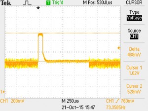
This is what one of the PCIe lane’s wires looks like when the PEX8606 switch is set to ignore the absence of receiver (with the SerDes X Mask Receiver Not Detected bit): It still runs the receiver detect test (the large pulse), but then goes to link training despite that no load was detected (that’s the noisy part after the pulse). In the shown case, the training kept failing (no response on the other side), so it goes back and forth between detection and training.

Oscilloscope plot of receiver detect of PLX8606

This capture was done with a plain digital oscilloscope (~ 200 MHz bandwidth).

PCIe: Xilinx’ pipe_clock module and its timing constraints

$
0
0

Introduction

In several versions of Xilinx’ wrapper for the integrated PCIe block, it’s the user application logic’s duty to instantiate the module which generates the “pipe clock”. It typically looks something like this:

pcie_myblock_pipe_clock #
      (
          .PCIE_ASYNC_EN                  ( "FALSE" ),                 // PCIe async enable
          .PCIE_TXBUF_EN                  ( "FALSE" ),                 // PCIe TX buffer enable for Gen1/Gen2 only
          .PCIE_LANE                      ( LINK_CAP_MAX_LINK_WIDTH ), // PCIe number of lanes
          // synthesis translate_off
          .PCIE_LINK_SPEED                ( 2 ),
          // synthesis translate_on
          .PCIE_REFCLK_FREQ               ( PCIE_REFCLK_FREQ ),        // PCIe reference clock frequency
          .PCIE_USERCLK1_FREQ             ( PCIE_USERCLK1_FREQ ),      // PCIe user clock 1 frequency
          .PCIE_USERCLK2_FREQ             ( PCIE_USERCLK2_FREQ ),      // PCIe user clock 2 frequency
          .PCIE_DEBUG_MODE                ( 0 )
      )
      pipe_clock_i
      (

          //---------- Input -------------------------------------
          .CLK_CLK                        ( sys_clk ),
          .CLK_TXOUTCLK                   ( pipe_txoutclk_in ),     // Reference clock from lane 0
          .CLK_RXOUTCLK_IN                ( pipe_rxoutclk_in ),
          .CLK_RST_N                      ( pipe_mmcm_rst_n ),      // Allow system reset for error_recovery
          .CLK_PCLK_SEL                   ( pipe_pclk_sel_in ),
          .CLK_PCLK_SEL_SLAVE             ( pipe_pclk_sel_slave),
          .CLK_GEN3                       ( pipe_gen3_in ),

          //---------- Output ------------------------------------
          .CLK_PCLK                       ( pipe_pclk_out),
          .CLK_PCLK_SLAVE                 ( pipe_pclk_out_slave),
          .CLK_RXUSRCLK                   ( pipe_rxusrclk_out),
          .CLK_RXOUTCLK_OUT               ( pipe_rxoutclk_out),
          .CLK_DCLK                       ( pipe_dclk_out),
          .CLK_OOBCLK                     ( pipe_oobclk_out),
          .CLK_USERCLK1                   ( pipe_userclk1_out),
          .CLK_USERCLK2                   ( pipe_userclk2_out),
          .CLK_MMCM_LOCK                  ( pipe_mmcm_lock_out)

      );

Consequently, some timing constraints that are related to the PCIe block’s internal functionality aren’t added automatically by the wrapper’s own constraints, but must be given explicitly by the user of the block, typically by following an example design.

This post discusses the implications of this situation. Obviously, none of this applies to PCIe block wrappers which handle this instantiation internally.

What is the pipe clock?

For our narrow purposes, the PIPE interface is the parallel data part of the SERDES attached to the Gigabit Transceivers (MGTs), which drive the physical PCIe lanes. For example, data to a Gen1 lane, running at 2.5 GT/s, requires 2.0 Gbit/s of payload data (as it’s expanded by a 10/8 ratio with 10b/8b encoding). If the SERDES is fed with 16 bits in parallel, a 125 MHz clock yields the correct data rate (125 MHz * 16 = 2 GHz).

By the same coin, a Gen2 interface requires a 250 MHz clock to support a payload data rate of 4.0 Gbit/s per lane (expanded into 5 GT/s with 10b/8b encoding).

The clock mux

If a PCIe block is configured for Gen2, it’s required to support both rates: 5 GT/s, and also be able to fall back to 2.5 GT/s if the link partner doesn’t support Gen2 or if the link doesn’t work properly at the higher rate.

In the most common setting (or always?), the pipe clock is muxed between two source clocks by this piece of code (in the pipe_clock module):

    //---------- PCLK Mux ----------------------------------
    BUFGCTRL pclk_i1
    (
        //---------- Input ---------------------------------
        .CE0                        (1'd1),
        .CE1                        (1'd1),
        .I0                         (clk_125mhz),
        .I1                         (clk_250mhz),
        .IGNORE0                    (1'd0),
        .IGNORE1                    (1'd0),
        .S0                         (~pclk_sel),
        .S1                         ( pclk_sel),
        //---------- Output --------------------------------
        .O                          (pclk_1)
    );
    end

So pclk_sel, which is a registered version of the CLK_PCLK_SEL input port is used to switch between a 125 MHz clock (pclk_sel == 0) and a 250 MHz clock (clk_sel == 1), both clocks generated from the same MMCM_ADV block in the pipe_clock module.

The BUFGMUX’ output, pclk_1 is assigned as the pipe clock output (CLK_PCLK). It’s also used in other ways, depending on the instantiation parameters of pipe_clock.

Constraints for Gen1 PCIe blocks

If a PCIe block is configured for Gen1 only, there’s no question about the pipe clock’s frequency: It’s 125 MHz. As a matter of fact, if the PCIE_LINK_SPEED instantiation parameter is set to 1, one gets (by virtue of Verilog’s generate commands)

    BUFG pclk_i1
    (
        //---------- Input ---------------------------------
        .I                          (clk_125mhz),
        //---------- Output --------------------------------
        .O                          (clk_125mhz_buf)
    );
    assign pclk_1 = clk_125mhz_buf;

But never mind this — it’s never used: Even when the block is configured as Gen1 only, PCIE_LINK_SPEED is set to 3 in the example design’s instantiation, and we all copy from it.

Instead, the clock mux is used and fed with pclk_sel=0. The constraints reflect this with the following lines appearing in the example design’s XDC file for Gen1 PCIe blocks (only!):

set_case_analysis 1 [get_pins {pcie_myblock_support_i/pipe_clock_i/pclk_i1_bufgctrl.pclk_i1/S0}]
set_case_analysis 0 [get_pins {pcie_myblock_support_i/pipe_clock_i/pclk_i1_bufgctrl.pclk_i1/S1}]
set_property DONT_TOUCH true [get_cells -of [get_nets -of [get_pins {pcie_myblock_support_i/pipe_clock_i/pclk_i1_bufgctrl.pclk_i1/S0}]]]

The first two commands tell the timing analysis tools to assume that the clock mux’ inputs are S0=1 and S1=0, and hence that the mux forwards the 125 MHz clock (connected to I0).

The DONT_TOUCH constraint works around a bug in early Vivado revisions, as explained in AR #62296: The S0 input is assigned ~pclk_sel, which requires a logic inverter. This inverter was optimized into the BUFCTRL primitive by the synthesizer, flipping the meaning of the first set_case_analysis constraints. Which caused the timing tools to analyze the design as if both S0 and S1 were set to zero, hence no clock output, and no constraining of the relevant paths.

The problem with this set of constraints is their cryptic nature: It’s not clear at all why they are there, just by reading the XDC file. If the user of the PCIe block decides, for example, to change from a 8x Gen1 configuration to 4x Gen2, everything will appear to work nicely, since all clocks except the pipe clock remain the same. It takes some initiative and effort to figure out that these constraints are incorrect for a Gen2 block.

To make things even worse, almost all relevant paths will meet the 250 MHz (4 ns) requirement even when constrained for 125 MHz on a sparsely filled FPGA, simply because there’s little logic along these paths. So odds are that everything will work fine during the initial tests (before the useful logic is added to the design), and later on the PCIe interface may become shaky throughout the design process, as some paths accidentally exceed the 4 ns limit.

Dropping the set_case_analysis constraints

As these constraints are relaxing by their nature, what happens if they are dropped? Once could expect that the tools would work a bit harder to ensure that all relevant paths meet timing with either 125 MHz or 250 MHz, or simply put, that the constraining would occur as if pclk_1 was always driven with a 250 MHz clock.

But this isn’t how timing calculations are made. The tools can’t just pick the faster clock from a clock mux and follow through, since the logic driven by the clock might interact with other clock domains. If so, a slower clock might require stricter timing due to different relations between the source and target clock’s frequencies.

So what actually happens is that the timing tools mark all logic driven by the pipe clock as having multiple clocks: The timing of each path going to and from any such logic element is calculated for each of the two clocks. Even the timing for paths going between logic elements that are both driven by the pipe clock are calculated four times, covering the four combinations of the 125 MHz and 250 MHz clocks, as source and destination clocks.

From a practical point of view, this is rather harmless, since both clocks come from the same MMCM_ADV, and are hence aligned. Making these excessive timing calculations always ends up with the equivalent for the 250 MHz clock only (some clock skew uncertainty possibly added for going between the two clocks). Since timing is met easily on these paths, this extra work adds very little to the implementation efforts (and how long it takes to finish).

On the other hand, this adds some dirt to the timing report. First, the multiple clocks are reported (excerpt from the Timing Report):

7. checking multiple_clock
--------------------------
 There are 2598 register/latch pins with multiple clocks. (HIGH)

Later on, the paths between logic driven by the pipe clock are counted as inter clock paths: Once from 125 MHz to 250 MHz, and vice versa. This adds up to a large number of bogus inter clock paths:

------------------------------------------------------------------------------------------------
| Inter Clock Table
| -----------------
------------------------------------------------------------------------------------------------

From Clock    To Clock          WNS(ns)      TNS(ns)  TNS Failing Endpoints  TNS Total Endpoints      WHS(ns)      THS(ns)  THS Failing Endpoints  THS Total Endpoints
----------    --------          -------      -------  ---------------------  -------------------      -------      -------  ---------------------  -------------------
clk_250mhz    clk_125mhz          0.114        0.000                      0                 5781        0.053        0.000                      0                 5781
clk_125mhz    clk_250mhz          0.114        0.000                      0                 5764        0.053        0.000                      0                 5764

Since a single endpoint might produce many paths (e.g. a block RAM), there’s no need for a correlation between the number of endpoints and the number of paths. However the similarity between the figures of the two directions seems to indicate that the vast majority of these paths are bogus.

So dropping the set_case_analysis constraints boils down to some noise in the timing report. I can think of two ways to eliminate it:

  • Issue set_case_analysis constraints setting S0=0, S1=1, so the tools assume a 250 MHz clock. This covers the Gen2 case as well as Gen1.
  • Use the constraints of the example design for a Gen2 block (shown below).

Even though both ways (in particular the second) seem OK to me, I prefer taking the dirt in the timing report and not add constraints without understanding the full implications. Being more restrictive never hurts (as long as the design meets timing).

Constraints for Gen2 PCIe blocks

If a PCIe block is configured for Gen2, it has to be able to work a Gen1 as well. So the set_case_analysis constraints are out of the question.

Instead, this is what one gets in the example design:

create_generated_clock -name clk_125mhz_x0y0 [get_pins pcie_myblock_support_i/pipe_clock_i/mmcm_i/CLKOUT0]
create_generated_clock -name clk_250mhz_x0y0 [get_pins pcie_myblock_support_i/pipe_clock_i/mmcm_i/CLKOUT1]
create_generated_clock -name clk_125mhz_mux_x0y0 \
                        -source [get_pins pcie_myblock_support_i/pipe_clock_i/pclk_i1_bufgctrl.pclk_i1/I0] \
                        -divide_by 1 \
                        [get_pins pcie_myblock_support_i/pipe_clock_i/pclk_i1_bufgctrl.pclk_i1/O]
#
create_generated_clock -name clk_250mhz_mux_x0y0 \
                        -source [get_pins pcie_myblock_support_i/pipe_clock_i/pclk_i1_bufgctrl.pclk_i1/I1] \
                        -divide_by 1 -add -master_clock [get_clocks -of [get_pins pcie_myblock_support_i/pipe_clock_i/pclk_i1_bufgctrl.pclk_i1/I1]] \
                        [get_pins pcie_myblock_support_i/pipe_clock_i/pclk_i1_bufgctrl.pclk_i1/O]
#
set_clock_groups -name pcieclkmux -physically_exclusive -group clk_125mhz_mux_x0y0 -group clk_250mhz_mux_x0y0

This may seem tangled, but says something quite simple: The 125 MHz and 250 MHz clocks are physically exclusive (see AR #58961 for an elaboration on this). In other words, these constraints declare that no path exists between logic driven by one clock and logic driven by the other. If such path is found, it’s bogus.

So this drops all the bogus paths mentioned above. Each path between logic driven by the pipe clock is now calculated twice (for 125 MHz and 250 MHz, but not across the clocks). This seems to yield the same practical results as without these constraints, but without complaints about multiple clocks, and of course no inter-clock paths.

Both clocks are still related to the pipe clock however. For example, checking a register driven by the pipe clock yields (Tcl session):

get_clocks -of_objects [get_pins -hier -filter {name=~*/pipe_clock_i/pclk_sel_reg1_reg[0]/C}]
clk_250mhz_mux_x0y0 clk_125mhz_mux_x0y0

Not surprisingly, this register is attached to two clocks. The multiple clock complaint disappeared thanks to the set_clock_groups constraint (even the lower “asynchronous” flag is enough for this purpose).

So can these constraints be used for a Gen1-only block, as a safer alternative for the set_case_analysis constraints? It seems so. Is it a good bargain for getting rid of those extra notes in the timing report? It’s a matter of personal choice. Or knowing for sure.

Bonus: Meaning of some instantiation parameters of pipe_clock

This is the meaning according to dissection of Kintex-7′s pipe_clock Verilog file. It’s probably the same for other targets.

PCIE_REFCLK_FREQ: The frequency of the reference clock

  • 1 => 125 MHz
  • 2 => 250 MHz
  • Otherwise: 100 MHz

CLKFBOUT_MULT_F is set to that the MCMM_ADV’s internal VCO always runs at 1 GHz. Hence the constant CLKOUT0_DIVIDE_F = 8 makes clk_125mhz run at 125 MHz (dividing by 8), and CLKOUT1_DIVIDE = 4 makes clk_250mhz run at 250 MHz (dividing by 8)

PCIE_USERCLK1_FREQ: The frequency of the module’s CLK_USERCLK1 output, which is among others the clock with the user interface (a.k.a. user_clk_out or axi_clk)

  • 1 => 31.25 MHz
  • 2 => 62.5 MHz
  • 3 => 125 MHz
  • 4 => 250 MHz
  • 5 => 500 MHz
  • Otherwise: 62.5 MHz

PCIE_USERCLK2_FREQ: The frequency of the module’s CLK_USERCLK2 output. Not used in most applications. Same frequency mapping as PCIE_USERCLK1_FREQ.

PCIe on Cyclone 10 GX: Data loss on DMA writes by FPGA

$
0
0

TL;DR

DMA writes from a Cyclone 10 GX PCIe interface may be lost, probably due to a path that isn’t timed properly by the fitter. This has been observed with Quartus Prime Version 17.1.0 Build 240 SJ Pro Edition, and the official Cyclone 10 GX development board. A wider impact is likely, possibly on Arria 10 device as well (as its PCIe block is the same one).

The problem seems to be rare, and appears and disappears depending on how the fitter places the logic. It’s however fairly easy to diagnose if this specific problem is in effect (see “The smoking gun” below).

Computer hardware: Gigabyte GA-B150M-D2V motherboard (with an Intel B150 Chipset) + Intel i5-6400 CPU.

The story

It started with a routine data transport test (FPGA to host), which failed virtually immediately (that is, after a few kilobytes). It was apparent that some portions of data simply weren’t written into the DMA buffer by the FPGA.

So I tried a fix in my own code, and yep, it helped. Or so I thought. Actually, anything I changed seemed to fix the problem. In the end, I changed nothing, but just added

set_global_assignment -name SEED 2

to the QSF file. Which only changes the fitter’s initial placement of the logic elements, which eventually leads to an alternative placement and routing of the design. That should work exactly the same, of course. But it “solved the problem”.

This was consistent: One “magic” build that failed consistently, and any change whatsoever made the issue disappear.

The design was properly constrained, of course, as shown in the development board’s sample SDC file. In fact, there isn’t much to constrain: It’s just setting the main clock to 100 MHz, derive_pll_clocks and derive_clock_uncertainty. And a false path from the PERST pin.

So maybe my bad? Well, no. There were no unconstrained paths in the entire design (with these simple constraints), so one fitting of the design should be exactly like any other. Maybe my application logic? No again:

The smoking gun

The final nail in the coffin was when I noted errors in the PCIe Device Status Registers on both sides. I’ve discussed this topic in this and this other posts of mine, however in the current case no AER kernel messages were produced (unfortunately, and it’s not clear why).

And whatever the application code does, Intel / Altera’s PCIe block shouldn’t produce a link error, and neither it does normally. It’s a violation of the PCIe spec.

These are the steps for observing this issue on a Linux machine. First, find out who the link partners are:

$ lspci
00:00.0 Host bridge: Intel Corporation Device 191f (rev 07)
00:01.0 PCI bridge: Intel Corporation Device 1901 (rev 07)
[ ... ]
01:00.0 Unassigned class [ff00]: Altera Corporation Device ebeb

and then figuring out that the FPGA card is connected via the bridge at 00:01.0 with

$ lspci -t
-[0000:00]-+-00.0
           +-01.0-[01]----00.0

So it’s between 00:01.0 and 01:00.0. Then, following that post of mine, using setpci to read from the status register to tell an error had occurred.

First, what it should look like: With any bitstream except that specific faulty one, I got

# setpci -s 01:00.0 CAP_EXP+0xa.w
0000
# setpci -s 00:01.0 CAP_EXP+0xa.w
0000

any time and all the time, which says the obvious: No errors sensed on either side.

But with the bitstream that had data losses, before any communication had taken place (except for the driver being loaded):

# setpci -s 01:00.0 CAP_EXP+0xa.w
0009
# setpci -s 00:01.0 CAP_EXP+0xa.w
0000

Non-zero means error. So at this stage the FPGA’s PCIe interface was unhappy with something (more on that below), but the processor’s side had no complaints.

I have to admit that I’ve seen the 0009 status in a lot of other tests, in which communication went through perfectly. So even though reflects some kind of error, it doesn’t necessarily predict any functional fault. As elaborated below, the 0009 status consists of correctable errors. It’s just that such errors are normally never seen (i.e. with any PCIe card that works properly).

Anyhow, back to the bitstream that did have data errors. After some data had been written by the FPGA:

# setpci -s 01:00.0 CAP_EXP+0xa.w
0009
# setpci -s 00:01.0 CAP_EXP+0xa.w
000a

In this case, the FPGA card’s link partner complained. To save ourselves the meaning of these numbers (even though the’re listed in that post), use lspci -vv:

# lspci -vv
00:01.0 PCI bridge: Intel Corporation Device 1901 (rev 07) (prog-if 00 [Normal decode])
[ ... ]
        Capabilities: [a0] Express (v2) Root Port (Slot+), MSI 00
                DevCap: MaxPayload 256 bytes, PhantFunc 0
                        ExtTag- RBE+
                DevCtl: Report errors: Correctable- Non-Fatal- Fatal- Unsupported-
                        RlxdOrd- ExtTag- PhantFunc- AuxPwr- NoSnoop-
                        MaxPayload 256 bytes, MaxReadReq 128 bytes
                DevSta: CorrErr- UncorrErr+ FatalErr- UnsuppReq+ AuxPwr- TransPend-
[ ... ]

So the bridge complained about an uncorrectable and an unsupported request only after the data transmission, but the FPGA side:

01:00.0 Unassigned class [ff00]: Altera Corporation Device ebeb
[ ... ]
        Capabilities: [80] Express (v2) Endpoint, MSI 00
                DevCap: MaxPayload 256 bytes, PhantFunc 0, Latency L0s <64ns, L1 <1us
                        ExtTag- AttnBtn- AttnInd- PwrInd- RBE+ FLReset-
                DevCtl: Report errors: Correctable- Non-Fatal- Fatal- Unsupported-
                        RlxdOrd+ ExtTag- PhantFunc- AuxPwr- NoSnoop+
                        MaxPayload 256 bytes, MaxReadReq 512 bytes
                DevSta: CorrErr+ UncorrErr- FatalErr- UnsuppReq+ AuxPwr- TransPend-

complained about a correctable error and an unsupported request (as seen above, that happened before any payload transmission).

Low-level errors. I couldn’t make this happen even if I wanted to.

Aftermath

The really bad news is that this problem isn’t in the logic itself, but in how it’s placed. It seems to be a rare and random occurrence of a poor job done by the fitter. Or maybe it’s not all that rare, if you let the FPGA heat up a bit. In my case a spinning fan kept an almost idle FPGA quite cool, I suppose.

The somewhat good news is that the data loss comes with these PCIe status errors, and maybe with the relevant kernel messages (not clear why I didn’t see any). So there’s something to hold on to.

And I should also mention that the offending PCIe interface was a Gen2 x 4 running with a 64-bit interface at 250 MHz. which a rather marginal frequency for Arria 10 / Cyclone 10. So going with the speculation that this is a timing issue that isn’t handled properly by the fitter, maybe sticking to 125 MHz interfaces on these devices is good enough to be safe against this issue.

Note to self: The outputs are kept in cyclone10-failure.tar.gz

Nvidia graphics cards on Linux: PCIe link speed and width

$
0
0

Why is it at 2.5 GT/s???

With all said about Nvidia’s refusal to release their drivers as open source, their Linux support is great. I don’t think I’ve ever had such a flawless graphics card experience with Linux. After replacing the nouveau driver with Nvidia’s, of course. Ideology is nice, but a computer that works is nicer.

But then I looked at the output of lspci -vv (on an Asus fanless GT 730 2GB DDR3), and horrors, it’s not running at full PCIe speed!

17:00.0 VGA compatible controller: NVIDIA Corporation GK208 [GeForce GT 730] (rev a1) (prog-if 00 [VGA controller])
        Subsystem: ASUSTeK Computer Inc. GK208B [GeForce GT 730]
[ ... ]
        Capabilities: [78] Express (v2) Legacy Endpoint, MSI 00
                DevCap: MaxPayload 256 bytes, PhantFunc 0, Latency L0s unlimited, L1 <64us
                        ExtTag+ AttnBtn- AttnInd- PwrInd- RBE+ FLReset-
                DevCtl: Report errors: Correctable- Non-Fatal- Fatal- Unsupported-
                        RlxdOrd+ ExtTag+ PhantFunc- AuxPwr- NoSnoop+
                        MaxPayload 256 bytes, MaxReadReq 512 bytes
                DevSta: CorrErr- UncorrErr- FatalErr- UnsuppReq- AuxPwr- TransPend-
                LnkCap: Port #0, Speed 5GT/s, Width x8, ASPM L0s L1, Exit Latency L0s <512ns, L1 <4us
                        ClockPM+ Surprise- LLActRep- BwNot- ASPMOptComp+
                LnkCtl: ASPM Disabled; RCB 64 bytes Disabled- CommClk+
                        ExtSynch- ClockPM+ AutWidDis- BWInt- AutBWInt-
                LnkSta: Speed 2.5GT/s, Width x8, TrErr- Train- SlotClk+ DLActive- BWMgmt- ABWMgmt-
[ ... ]
        Kernel driver in use: nvidia
        Kernel modules: nvidiafb, nouveau, nvidia_drm, nvidia

Whatwhat? The card declares it supports 5 GT/s, but runs only at 2.5 GT/s? And on my brand new super-duper motherboard, which supports Gen3 PCIe connected directly to an Intel X-family CPU?

It’s all under control

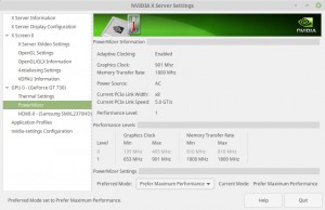
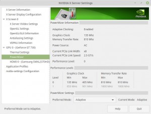
Well, the answer is surprisingly simple: Nvidia’s driver changes the card’s PCIe speed dynamically to support the bandwidth needed. When there’s no graphics activity, the speed drops to 2.5 GT/s.

This behavior can be controlled with Nvidia’s X Server Settings control panel (it has an icon in the system’s setting panel, or just type “Nvidia” on Gnome’s start menu). Under the PowerMizer sub-menu, the card’s behavior can be changed to stay at 5 GT/s if you like your card hot and electricity bill fat.

Otherwise, in “Adaptive mode” it switches back and forth from 2.5 GT/s to 5 GT/s. The screenshot below was taken after a few seconds of idling (click to enlarge):

Screenshot of Nvidia X Server settings in adaptive mode

And this is how to force it to 5 GT/s constantly (click to enlarge):

Screenshot of Nvidia X Server settings in maximum performance mode

With the latter setting, lspci -vv shows that the card is at 5 GT/s, as promised:

17:00.0 VGA compatible controller: NVIDIA Corporation GK208 [GeForce GT 730] (rev a1) (prog-if 00 [VGA controller])
        Subsystem: ASUSTeK Computer Inc. GK208B [GeForce GT 730]
[ ... ]
                LnkCap: Port #0, Speed 5GT/s, Width x8, ASPM L0s L1, Exit Latency L0s <512ns, L1 <4us
                        ClockPM+ Surprise- LLActRep- BwNot- ASPMOptComp+
                LnkCtl: ASPM Disabled; RCB 64 bytes Disabled- CommClk+
                        ExtSynch- ClockPM+ AutWidDis- BWInt- AutBWInt-
                LnkSta: Speed 5GT/s, Width x8, TrErr- Train- SlotClk+ DLActive- BWMgmt- ABWMgmt-

So don’t worry about a low speed on an Nvidia card (or make sure it steps up on request).

A word on GT 1030

I added another fanless card, Asus GT 1030 2GB, to the computer for some experiments. This card is somewhat harder to catch at 2.5 GT/s, because it steps up very quickly in response to any graphics event. But I managed to catch this:

65:00.0 VGA compatible controller: NVIDIA Corporation GP108 (rev a1) (prog-if 00 [VGA controller])
        Subsystem: ASUSTeK Computer Inc. GP108 [GeForce GT 1030]
[ ... ]
                LnkCap: Port #0, Speed 8GT/s, Width x4, ASPM L0s L1, Exit Latency L0s <512ns, L1 <16us
                        ClockPM+ Surprise- LLActRep- BwNot- ASPMOptComp+
                LnkCtl: ASPM Disabled; RCB 64 bytes Disabled- CommClk+
                        ExtSynch- ClockPM+ AutWidDis- BWInt- AutBWInt-
                LnkSta: Speed 2.5GT/s, Width x4, TrErr- Train- SlotClk+ DLActive- BWMgmt- ABWMgmt-

The running 2.5 GT/s speed vs. the maximal 8 GT/s is pretty clear by now, but the declared maximal Width is 4x? If so, why does it have a 16x PCIe form factor? The GT 730 has an 8x form factor, and uses 8x lanes, but GT 1030 has 16x and declares it can only use 4x? Is this some kind of marketing thing to make the card look larger and stronger?

On the other hand, show me a fairly recent motherboard without a 16x PCIe slot. The thing is that sometimes that slot can be used for something else, and the graphics card could then have gone into a vacant 4x slot instead. But no. Let’s make it big and impressive with a long PCIe plug that makes it look massive. Personally, I find the gigantic heatsink impressive enough.


Intel FPGA’s Stratix 10: My impressions and notes

$
0
0

Introduction

These are a few random things I wrote down as I worked with the Stratix 10 Development Kit, with focus on its PCIe interface. Quite obviously, it’s mostly about things I found noteworthy about this specific FPGA and its board, compared with previous hardware I’ve encountered.

Generally speaking, Stratix 10 is not for the faint-hearted: It has quite a few special issues that require attention when designing with it (some detailed below), and it’s clearly designed with the assumption that if you’re working with this king-sized beast, you’re most likely part of some high-end project, being far from a novice in the FPGA field.

Some National Geographic

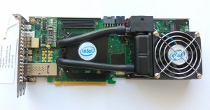
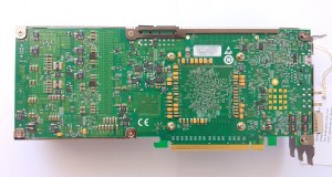
Even though I discuss the development kit further below, I’ll start with a couple of images of the board’s front and back. This 200W piece of logic has a liquid cooler and an exceptionally noisy fan — none of which are shown in Intel’s official images I’ve seen. In other words, it’s not as innocent as it may appear from the official pics.

There are no earplugs in the kit itself, so it’s recommended to buy something of that sort along with it. One could only wish for a temperature controlled fan. I mean, measuring the temperature of the liquid would probably have done the job. Some silence when the device isn’t working hard.

So here’s what the board looks like out of the box (in particular DIP switches in the default positions). Click images to enlarge.

Front side of Stratix 10 Development Kit

Front side of Stratix 10 Development Kit

Back side of Stratix 10 Development Kit

Back side of Stratix 10 Development Kit


“Hyperflex”

The logic on the Stratix 10 FPGAs has been given this rather promising name, implying that there’s something groundbreaking about it. However synthesizing a real-life design for Stratix 10, I experienced no advantage over Cyclone 10: All of the hyper-something phases got their moment of glory during the project implementation (Quartus Pro 19.2), but frankly speaking, when the design got the slightest heavy (5% of the FPGA resources, but still a 256-bit wide bus everywhere on a 250 MHz clock), timing failed exactly as it would on a Cyclone 10.

Comparing with Xilinx, it feels a bit like Kintex-7 (mainline speed grade -2), in terms of the logic’s timing performance. Maybe if the logic design is tuned to fit the architecture, there’s a difference.

Assuming that this Hyperflex thing is more than just a marketing buzz, I imagine that the features of this architecture are taken advantage of in Intel’s own IP cores for certain tasks (with extensive pipelining?). Just don’t expect anything hyper to happen when implementing your own plain design.

PCIe, Transceivers and Tiles

It’s quite common to use the term “tiles” in the FPGA industry to describe sections on the silicon die that belong to a certain functionality. However the PCIe + transceiver tiles on a Stratix 10 are separate silicon dies on the package substrate, connected to the main logic fabric (“HyperFlex”) through Intel’s Embedded Multi-die Interconnect Bridge (EMIB) interface. Not that it really matters, but anyhow.

H, L and E tiles provide Gigabit transceivers. H and L tiles come with exactly one PCIe hard IP each, E-tiles with 100G Ethernet. There might be one or more of these tiles on a Stratix 10 device. It seems like the L tile will vanish with time, as it has weaker performance in almost all parameters.

All tiles have 24 Gigabit transceivers. Those not used by the hard IP are vacant for general purpose, even though some might become unusable, subject to certain rules (given in the relevant user guides).

And here comes the hard nut: PCIe has a minimal data interface of 256 bits with the application logic. The other possibility is 512 bits. This can be a significant burden when porting a design from earlier FPGA families, in particular if they were based upon a narrower data interface.

Xillybus supports the Stratix 10 device family, however.

PCIe unsupported request error

Quite interestingly, there were correctable (and hence practically harmless) errors on the PCIe link consistently when booting a PC with the official development kit, with a production grade (i.e. not ES) H-tile FPGA. This is what plain lspci -vv gave me, even before the application logic got a chance to do anything:

01:00.0 Unassigned class [ff00]: Altera Corporation Device ebeb (rev 01)
        Subsystem: Altera Corporation Device ebeb
        Control: I/O- Mem+ BusMaster- SpecCycle- MemWINV- VGASnoop- ParErr- Stepping- SERR- FastB2B- DisINTx-
        Status: Cap+ 66MHz- UDF- FastB2B- ParErr- DEVSEL=fast >TAbort- <TAbort- <MAbort- >SERR- <PERR- INTx-
        Interrupt: pin A routed to IRQ 16
        Region 0: Memory at d0100000 (64-bit, prefetchable) [size=256]
        Capabilities: [40] Power Management version 3
                Flags: PMEClk- DSI- D1- D2- AuxCurrent=0mA PME(D0-,D1-,D2-,D3hot-,D3cold-)
                Status: D0 NoSoftRst- PME-Enable- DSel=0 DScale=0 PME-
        Capabilities: [50] MSI: Enable- Count=1/1 Maskable+ 64bit-
                Address: 00000000  Data: 0000
                Masking: 00000000  Pending: 00000000
        Capabilities: [70] Express (v2) Endpoint, MSI 00
                DevCap: MaxPayload 512 bytes, PhantFunc 0, Latency L0s <64ns, L1 <1us
                        ExtTag- AttnBtn- AttnInd- PwrInd- RBE+ FLReset+
                DevCtl: Report errors: Correctable- Non-Fatal- Fatal- Unsupported-
                        RlxdOrd+ ExtTag- PhantFunc- AuxPwr- NoSnoop- FLReset-
                        MaxPayload 256 bytes, MaxReadReq 512 bytes
                DevSta: CorrErr+ UncorrErr- FatalErr- UnsuppReq+ AuxPwr- TransPend-
                LnkCap: Port #1, Speed 5GT/s, Width x16, ASPM not supported, Exit Latency L0s <64ns, L1 <1us
                        ClockPM- Surprise- LLActRep- BwNot-
                LnkCtl: ASPM Disabled; RCB 64 bytes Disabled- CommClk-
                        ExtSynch- ClockPM- AutWidDis- BWInt- AutBWInt-
                LnkSta: Speed 5GT/s, Width x16, TrErr- Train- SlotClk- DLActive- BWMgmt- ABWMgmt-
                DevCap2: Completion Timeout: Range ABCD, TimeoutDis+, LTR-, OBFF Not Supported
                DevCtl2: Completion Timeout: 50us to 50ms, TimeoutDis-, LTR-, OBFF Disabled
                LnkCtl2: Target Link Speed: 5GT/s, EnterCompliance- SpeedDis-
                         Transmit Margin: Normal Operating Range, EnterModifiedCompliance- ComplianceSOS-
                         Compliance De-emphasis: -6dB
                LnkSta2: Current De-emphasis Level: -6dB, EqualizationComplete-, EqualizationPhase1-
                         EqualizationPhase2-, EqualizationPhase3-, LinkEqualizationRequest-
        Capabilities: [100 v2] Advanced Error Reporting
                UESta:  DLP- SDES- TLP- FCP- CmpltTO- CmpltAbrt- UnxCmplt- RxOF- MalfTLP- ECRC- UnsupReq- ACSViol-
                UEMsk:  DLP- SDES- TLP- FCP- CmpltTO- CmpltAbrt- UnxCmplt- RxOF- MalfTLP- ECRC- UnsupReq- ACSViol-
                UESvrt: DLP+ SDES+ TLP- FCP+ CmpltTO- CmpltAbrt- UnxCmplt- RxOF+ MalfTLP+ ECRC- UnsupReq- ACSViol-
                CESta:  RxErr- BadTLP- BadDLLP- Rollover- Timeout- NonFatalErr+
                CEMsk:  RxErr- BadTLP- BadDLLP- Rollover- Timeout- NonFatalErr+
                AERCap: First Error Pointer: 00, GenCap+ CGenEn- ChkCap+ ChkEn-

As highlighted above, Unsupported Request correctable errors took place on the link. Even though this is harmless, it’s nevertheless nothing that should happen on a properly working PCIe link.

Note that I ran the PCIe link on Gen2 only, even though it supports Gen3. Not that it should matter.

Reset release IP

According to Intel’s Configuration Guide for Stratix 10 for Quartus Design Suite 19.2, one can’t rely on the device’s consistent wakeup, but the nINIT_DONE signal must be used to reset all logic:

“The entire device does not enter user mode simultaneously. Intel requires you to include the Intel Stratix 10 Reset Release IP on page 22 to hold your application logic in the reset state until the entire FPGA fabric is in user mode. Failure to include this IP in your design may result in intermittent application logic failures.”

Note nINIT_DONE is asserted (low) when it’s fine to run the logic, so it’s effective an active HIGH reset. It’s so easy to get confused, as the “n” prefix triggers the “active low reset” part of an FPGA designer’s brain.

Failing to have the Reset Release IP included in the project results the following critical warning during synthesis (Quartus Pro 19.2):

Critical Warning (20615): Use the Reset Release IP in Intel Stratix 10 designs to ensure a successful configuration. For more information about the Reset Release IP, refer to the Intel Stratix 10 Configuration User Guide.

The IP just exposes the nINIT_DONE signal as an output and has no parameters. It boils down to the following:

wire ninit_done;
altera_s10_user_rst_clkgate init_reset(.ninit_done(ninit_done));

One could instantiate this directly, but it’s not clear if this is Quartus forward compatible, and it won’t silence the critical warning.

However Quartus Pro 18.0 doesn’t issue any warning if the Reset Release IP is missing, and neither is this issue mentioned in the related configuration guide. Actually, the required IP isn’t available on Quartus Pro 18.0. This issue obviously evolved with time.

Variable core voltage (SmartVID)

Another ramp-up in the usage complexity is the core voltage supply. The good old practice is to set the power supply to whatever voltage the datasheet requires, but no, Stratix 10 FPGAs need to control the power supply, in order to achieve the exact voltage that is required for each specific device. So there’s now a Power Management User Guide to tackle this issue.

This has a reason: As the transistors get smaller, so does the tolerance of the process get a larger impact. To compensate for these tolerances, and not take a hit on the timing performance, each device has its own ideal core voltage. So if you’ve gone as far as using a Stratix 10 FPGA, what’s connecting a few I2C wires to the power supply and let it pick its favorite voltage?

The impact on the FPGA design is the need to inform the tools which pins to use for this purpose, what I2C address to use, which power supply to expect on the other end, and other parameters. This takes the form of a few extra lines, as shown below for the Stratix 10 Development Kit:

set_global_assignment -name USE_PWRMGT_SCL SDM_IO14
set_global_assignment -name USE_PWRMGT_SDA SDM_IO11
set_global_assignment -name VID_OPERATION_MODE "PMBUS MASTER"
set_global_assignment -name PWRMGT_BUS_SPEED_MODE "400 KHZ"
set_global_assignment -name PWRMGT_SLAVE_DEVICE_TYPE LTM4677
set_global_assignment -name PWRMGT_SLAVE_DEVICE0_ADDRESS 4F
set_global_assignment -name PWRMGT_SLAVE_DEVICE1_ADDRESS 00
set_global_assignment -name PWRMGT_SLAVE_DEVICE2_ADDRESS 00
set_global_assignment -name PWRMGT_SLAVE_DEVICE3_ADDRESS 00
set_global_assignment -name PWRMGT_SLAVE_DEVICE4_ADDRESS 00
set_global_assignment -name PWRMGT_SLAVE_DEVICE5_ADDRESS 00
set_global_assignment -name PWRMGT_SLAVE_DEVICE6_ADDRESS 00
set_global_assignment -name PWRMGT_SLAVE_DEVICE7_ADDRESS 00
set_global_assignment -name PWRMGT_PAGE_COMMAND_ENABLE ON
set_global_assignment -name PWRMGT_VOLTAGE_OUTPUT_FORMAT "AUTO DISCOVERY"
set_global_assignment -name PWRMGT_TRANSLATED_VOLTAGE_VALUE_UNIT VOLTS

It’s among the things that are easy when they work, but when designing your own board and something goes wrong with the I2C bus, well, well.

“Self service licensing”

The Stratix 10 Development Kit includes a one-year license for Quartus Pro, which is activated on Intel’s website. It’s recommended to start this process as soon as possible, as it has a potential of getting tangled and time consuming. In particular, be sure to know which email address was reported to Intel along with the purchase of the Kit, and that you have a fully verified account for that email address on Intel’s website.

That’s because the self-service licensing procedure is possible only from the Intel account that is registered with a specific email address. This email address is the one that the distributor reported when forwarding the order for the development kit to Intel. In my case, they used an address they had on record from a previous purchase I made from the same distributor, and it didn’t even cross my mind to try it.

Be sure to fill in the detailed registration form and to confirm the email address. Access to the licensing area is denied otherwise. It continues to be denied for a few days after filling in the details. Probably a matter of validation by a human.

The serial number that needs to be fed in (or does it? see below) is the one that appears virtually everywhere (on the PCB itself, on the package, on the outer box with which the package arrived), and has the form of e.g. 10SHTPCIe0001234. However the instructions said it should be “printed on the side of the development kit box below the bottom bar code”. Well, there is nothing printed under the bottom bar code. It’s not so difficult to find it, as it says “serial number”, but when the registration fails, this misleading direction adds a level of confusion.

Since the serial number is so out in the open, it’s quite clear why another form of authentication is needed. Too bad that the email issue wasn’t mentioned in the instructions.

In my case, there was no need to feed any serial number. Once the Intel account was validated (a few days after filling in the registration details), the license simply appeared on the self-service licensing page. As I contacted Intel’s licensing support twice throughout the process, it’s possible that someone at Intel’s support took care of pairing the serial number  with my account.

Development kit’s power supplies

I put this section last, because it’s the one that is quite pointless reading, frankly speaking. The bottom line is simple, exactly like the user guide says: If you use the board stand-alone, use the power supply that came along with it. If the board goes into the PCIe slot, connect both J26 and J27 to the computer’s ATX power supply, or the board will not power up.

J27 is a plain PCIe power connector (6 pins), and J26 is an 8-pin power connector. On my plain ATX power supply there was a PCIe power connector with a pair of extra pins attached with a cable tie (8 pins total). It fit in nicely into J26, it worked, no smoke came out, so I guess that’s the way it should be done. See pictures below, click to enlarge.

ATX power supply connected to Stratix 10 Development Kit, front side

ATX power supply connected to Stratix 10 Development Kit, front side

ATX power supply connected to Stratix 10 Development Kit, back side

ATX power supply connected to Stratix 10 Development Kit, back side

Now to the part you can safely skip:

As the board is rated at 240 W and may draw up to 20A from its internal +12V power supply, it might be interesting understand how the power load is distributed among the different sources. However the gory details have little practical importance, as the board won’t power up when plugged in as a PCIe card unless power is applied both to J26 and J27 (the power-up is sequencer set up this way, I guess). So this is just a little bit of theory.

There are three power groups, each having a separate 12V power rail: 12V_GROUP1, 12V_GROUP2 and 12V_GROUP3.

12V_GROUP2 will feed 12V_GROUP1 and 12V_GROUP3 with current if their voltage is lower than its own, by virtue of an emulated ideal diode. It’s as if there was two ideal diodes connected with their anodes on 12V_GROUP2 and one diode’s cathode on 12V_GROUP1, and cathode on 12V_GROUP3.

These voltage rails are in turn fed by external connectors, through emulated ideal diodes as follows:

  • J26 (8-pin aux voltage) feeds 12V_GROUP1
  • J27 (6-pin PCIe / power brick) feeds 12V_GROUP2
  • The PCIe slot’s 12V supply feeds 12V_GROUP3

The PCIe slot’s 3.3V supply is not used by the board.

This arrangement makes sense: If the board is used standalone, the brick power supply is connected to J27, and feeds all three groups. When used in a PCIe slot, the slot itself can only power 12V_GROUP3, so by itself, the board can’t power up. Theoretically speaking, J27 needs to be connected to the computer’s power supply through a PCIe power connector, at the very least. For the higher power applications, J26 should be connected as well to the power supply, to allow for the higher current flow. In practice, J27 alone won’t power the board up, probably as a safety measure.

The FPGA’s core voltage is S10_VCC, which is generated from 12V_GROUP1 — this is the heavy lifting, and it’s not surprising that it’s connected to J26, which is intended for the higher currents.

The ideal diode emulation is done with LTC4357 devices, which measure the voltage between the emulated diode’s anode and cathode. If this voltage is slightly positive, the device opens a external power FET by applying voltage to its gate. This FET’s drain and source pins are connected to the emulated diode’s anode and cathode pins, so all in all, when there’s a positive voltage across it, current flows. This reduces the voltage drop considerably, allowing efficient power supply OR-ing, as done extensively on this development kit.

The board’s user guide advises against connecting the brick power supply to J27 when the board is in a PCIe slot, but also mentions the ideal diode mechanism (once again, it won’t power up at all this way). This is understandable, as doing so will cause current to be drawn from the PCIe slot’s 12V supply when its voltage is higher that the one supplied by J27, even momentarily. With the voltage turbulence that is typical to switching power supplies, the currents may end up swinging quite a lot in an unfortunate combination of power supplies.

So even though it’s often more comfortable to control the power of the board separately from the hosting computer’s power, or to connect J27 only if the board is expected to draw less than 75W, both possibilities are eliminated. Both the noisy fan and the board’s refusal to power up unless fed properly prepare the board for the worst case power consumption scenario.

Critical Warnings after upgrading a PCIe block for Ultrascale+ on Vivado 2020.1

$
0
0

Introduction

Checking Xillybus’ bundle for Kintex Ultrascale+ on Vivado 2020.1, I got several critical warnings related to the PCIe block. As the bundle is intended to show how Xillybus’ IP core is used for simplifying communication with the host, these warnings aren’t directly related, and yet they’re unacceptable.

This bundle is designed to work with Vivado 2017.3 and later: It sets up the project by virtue of a Tcl script, which among others calls the upgrade_ip function for updating all IPs. Unfortunately, a bug in Vivado 2020.1 (and possibly other versions) causes the upgraded PCIe block to end up misconfigured.

This bug applies to Zynq Ultrascale+ as well, but curiously enough not with Virtex Ultrascale+. At least with my setting there was no problem.

The problem

Having upgraded an UltraScale+ Integrated Block (PCIE4) for PCI Express IP block from Vivado 2017.3 (or 2018.3) to Vivado 2020.1, I got several Critical Warnings. Three during synthesis:

[Vivado 12-4739] create_clock:No valid object(s) found for '-objects [get_pins -filter REF_PIN_NAME=~TXOUTCLK -of_objects [get_cells -hierarchical -filter {NAME =~ *gen_channel_container[1200].*gen_gtye4_channel_inst[3].GT*E4_CHANNEL_PRIM_INST}]]'. ["project/pcie_ip_block/source/ip_pcie4_uscale_plus_x0y0.xdc":127]
[Vivado 12-4739] get_clocks:No valid object(s) found for '--of_objects [get_pins -hierarchical -filter {NAME =~ *gen_channel_container[1200].*gen_gtye4_channel_inst[3].GTYE4_CHANNEL_PRIM_INST/TXOUTCLK}]'. ["project/pcie_ip_block/synth/pcie_ip_block_late.xdc":63]
[Vivado 12-4739] get_clocks:No valid object(s) found for '--of_objects [get_pins -hierarchical -filter {NAME =~ *gen_channel_container[1200].*gen_gtye4_channel_inst[3].GTYE4_CHANNEL_PRIM_INST/TXOUTCLK}]'. ["project/pcie_ip_block/synth/pcie_ip_block_late.xdc":64]

and another seven during implementation:

[Vivado 12-4739] create_clock:No valid object(s) found for '-objects [get_pins -filter REF_PIN_NAME=~TXOUTCLK -of_objects [get_cells -hierarchical -filter {NAME =~ *gen_channel_container[1200].*gen_gtye4_channel_inst[3].GT*E4_CHANNEL_PRIM_INST}]]'. ["project/pcie_ip_block/source/ip_pcie4_uscale_plus_x0y0.xdc":127]
[Vivado 12-4739] set_clock_groups:No valid object(s) found for '-group [get_clocks -of_objects [get_pins -hierarchical -filter {NAME =~ *gen_channel_container[1200].*gen_gtye4_channel_inst[3].GTYE4_CHANNEL_PRIM_INST/TXOUTCLK}]]'. ["project/pcie_ip_block/synth/pcie_ip_block_late.xdc":63]
[Vivado 12-4739] set_clock_groups:No valid object(s) found for '-group '. ["project/pcie_ip_block/synth/pcie_ip_block_late.xdc":63]
[Vivado 12-4739] set_clock_groups:No valid object(s) found for '-group [get_clocks -of_objects [get_pins -hierarchical -filter {NAME =~ *gen_channel_container[1200].*gen_gtye4_channel_inst[3].GTYE4_CHANNEL_PRIM_INST/TXOUTCLK}]]'. ["project/pcie_ip_block/synth/pcie_ip_block_late.xdc":64]
[Vivado 12-4739] set_clock_groups:No valid object(s) found for '-group '. ["project/pcie_ip_block/synth/pcie_ip_block_late.xdc":64]
[Vivado 12-5201] set_clock_groups: cannot set the clock group when only one non-empty group remains. ["project/pcie_ip_block/synth/pcie_ip_block_late.xdc":63]
[Vivado 12-5201] set_clock_groups: cannot set the clock group when only one non-empty group remains. ["project/pcie_ip_block/synth/pcie_ip_block_late.xdc":64]

The first warning in each group points at this line in ip_pcie4_uscale_plus_x0y0.xdc, which was automatically generated by the tools:

create_clock -period 4.0 [get_pins -filter {REF_PIN_NAME=~TXOUTCLK} -of_objects [get_cells -hierarchical -filter {NAME =~ *gen_channel_container[1200].*gen_gtye4_channel_inst[3].GT*E4_CHANNEL_PRIM_INST}]]

And the other at these two lines in pcie_ip_block_late.xdc, also generated by the tools:

set_clock_groups -asynchronous -group [get_clocks -of_objects [get_ports sys_clk]] -group [get_clocks -of_objects [get_pins -hierarchical -filter {NAME =~ *gen_channel_container[1200].*gen_gtye4_channel_inst[3].GTYE4_CHANNEL_PRIM_INST/TXOUTCLK}]]
set_clock_groups -asynchronous -group [get_clocks -of_objects [get_pins -hierarchical -filter {NAME =~ *gen_channel_container[1200].*gen_gtye4_channel_inst[3].GTYE4_CHANNEL_PRIM_INST/TXOUTCLK}]] -group [get_clocks -of_objects [get_ports sys_clk]]

So this is clearly about a reference to a non-existent logic cell supposedly named gen_channel_container[1200], and in particular that index, 1200, looks suspicious.

I would have been relatively fine with ignoring these warnings had it been just the set_clock_groups that failed, as these create false paths. If the design implements properly without these, it’s fine. But failing a create_clock command is serious, as this can leave paths unconstrained. I’m not sure if this is indeed the case, and it doesn’t matter all that much. One shouldn’t get used to ignoring critical warnings.

Looking at the .xci file for this PCIe block, it’s apparent that several changes were made to it while upgrading to 2020.1. Among those changes, these three lines were added:

<spirit:configurableElementValue spirit:referenceId="MODELPARAM_VALUE.MASTER_GT">GTHE4_CHANNEL_X49Y99</spirit:configurableElementValue>
<spirit:configurableElementValue spirit:referenceId="MODELPARAM_VALUE.MASTER_GT_CONTAINER">1200</spirit:configurableElementValue>
<spirit:configurableElementValue spirit:referenceId="MODELPARAM_VALUE.MASTER_GT_QUAD_INX">3</spirit:configurableElementValue>

Also, somewhere else in the XCI file, this line was added:

<spirit:configurableElementValue spirit:referenceId="PARAM_VALUE.MASTER_GT">GTHE4_CHANNEL_X49Y99</spirit:configurableElementValue>

So there’s a bug in the upgrading mechanism, which sets some internal parameter to select the a nonexistent GT site.

The manual fix (GUI)

To rectify the wrong settings manually, enter the settings of the PCIe block, and click the checkbox for “Enable GT Quad Selection” twice: Once for unchecking, and once for checking it. Make sure that the selected GT hasn’t changed.

Then it might be required to return some unrelated settings to their desired values. In particular, the PCI Device ID and similar attributes change to Xilinx’ default as a result of this. It’s therefore recommended to make a copy of the XCI file before making this change, and then use a diff tool to compare the before and after files, looking for irrelevant changes. Given that this revert to default has been going on for so many years, it seems like Xilinx considers this a feature.

But this didn’t solve my problem, as the bundle needs to set itself correctly out of the box.

Modifying the XCI file? (Not)

The immediate thing to check was whether this problem applies to PCIe blocks that are created in Vivado 2020.1 from scratch inside a project which is set to target KCU116 (which is what the said Xillybus bundle targets). As expected, it doesn’t — this occurs just on upgraded IP blocks: With the project that was set up from scratch, the related lines in the XCI file read:

<spirit:configurableElementValue spirit:referenceId="MODELPARAM_VALUE.MASTER_GT">GTYE4_CHANNEL_X0Y7</spirit:configurableElementValue>
<spirit:configurableElementValue spirit:referenceId="MODELPARAM_VALUE.MASTER_GT_CONTAINER">1</spirit:configurableElementValue>
<spirit:configurableElementValue spirit:referenceId="MODELPARAM_VALUE.MASTER_GT_QUAD_INX">3</spirit:configurableElementValue>

and

<spirit:configurableElementValue spirit:referenceId="PARAM_VALUE.MASTER_GT">GTYE4_CHANNEL_X0Y7</spirit:configurableElementValue>

respectively. These are values that make sense.

With this information at hand, my first attempt to solve this was to add the four new lines to the old XCI file. This allowed using the XCI file with Vivado 2020.1 properly, however synthesizing the PCIe block on older Vivado versions failed: As it turns out, all MODELPARAM_VALUE attributes become instantiation parameters for pcie_uplus_pcie4_uscale_core_top inside the PCIe block. However looking at the source file (on 2020.1), these parameters are indeed defined (only in those generated in 2020.1), and yet they are unused, like many other instantiation parameters in this module. So apparently, Vivado’s machinery generates an instantiation parameter for each of these, even if they’re not used. Those unused parameters are most likely intended for scripting.

So this trick made Vivado instantiate the pcie_uplus_pcie4_uscale_core_top with instantiation parameters that it doesn’t have, and hence its synthesis failed. Dead end.

I didn’t examine the possibility to deselect “Enable GT Quad Selection” in the original block, because Vivado 2017.3 chooses the wrong GT for the board without this option.

Workaround with Tcl

Eventually, I solved the problem by adding a few lines to the Tcl script.

Assuming that $ip_name has been set to the name of the PCIe block IP, this Tcl snippet rectifies the bug:

if {![string equal "" [get_property -quiet CONFIG.MASTER_GT [get_ips $ip_name]]]} {
  set_property -dict [list CONFIG.en_gt_selection {true} CONFIG.MASTER_GT {GTYE4_CHANNEL_X0Y7}] [get_ips $ip_name]
}

This snippet should of course be inserted after updating the IP core (with e.g. upgrade_ip [get_ips]). The code first checks if the MASTER_GT is defined, and only if so, it sets it to the desired value. This ensures that nothing happens with the older Vivado versions. Note the “quiet” flag of get_properly, which prevents it from generating an error if the property isn’t defined. Rather, it returns an empty string if that’s the case, which is what the result is compared against.

Setting MASTER_GT this way also rectifies GT_CONTAINER correctly, and surprisingly enough, this doesn’t change anything it shouldn’t, and in particular, the Device IDs remain intact.

However the disadvantage with this solution is that the GT to select is hardcoded in the Tcl code. But that’s fine in my case, for which a specific board (KCU116) is targeted by the bundle.

Another way to go, which is less recommended, is to emulate the check and uncheck of “Enable GT Quad Selection”:

if {![string equal "" [get_property -quiet CONFIG.MASTER_GT [get_ips $ip_name]]]} {
  set_property CONFIG.en_gt_selection {false} [get_ips $ip_name]
  set_property CONFIG.en_gt_selection {true} [get_ips $ip_name]
}

However turning the en_gt_selection flag off and on again also resets the Device ID to default as with manual toggling of the checkbox. And even though it set the MASTER_GT correctly in my specific case, I’m not sure whether this can be relied upon.

Viewing all 30 articles
Browse latest View live


<script src="https://jsc.adskeeper.com/r/s/rssing.com.1596347.js" async> </script>